
Current status and challenges in microchip research
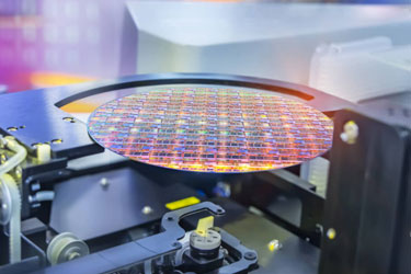
In this day and age, a microchip is capable of integrating an extremely large number of transistors, tens of billions or more. The manufacturing process is extremely complex and delicate, yet the accurate characterization and mapping of the resulting structures faces enormous difficulties. Although scanning electron microscopes are capable of resolutions of a few nanometers, which makes them ideally suited to imaging microtransistors, this technique typically only produces two-dimensional images of the surface of an object. To obtain a three-dimensional image, the chip must be examined layer by layer, which inevitably destroys the structure of the chip.
X-ray Technology for Microchip Research
X-rays have the property of penetrating deeper into materials, and X-ray tomography can theoretically be used to generate three-dimensional images without destroying the chip. However, existing X-ray technology is not adequate for accurately imaging microscopic structures such as microchips.
Solutions and technological innovations
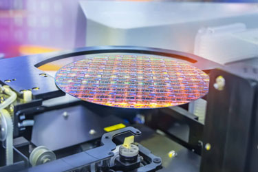
To overcome this challenge, a team of scientists from the Paul Scherrer Institute in Switzerland, the Ecole Polytechnique Fédérale de Lausanne (EPFL), the ETH Zurich, and the University of Southern California (USC) have adopted stacked coherent diffraction imaging as a solution.
The unique feature of this technique is that instead of focusing the X-ray beam on a nanometer point on the sample, the sample is moved around on a nanometer scale so that the path of the X-ray beam illuminating the sample forms a precise grid. Each point on the grid records the diffraction pattern of the sample, and because the distance between individual grid points is smaller than the beam diameter, the imaging areas overlap, thus providing enough information to allow algorithms to reconstruct the image of the sample at high resolution.
Technological breakthroughs and future applications
In 2017, the research team successfully imaged a computer chip in space with a resolution of 15 nanometers, setting a record at the time. Since then, they have been working tirelessly to improve the accuracy of this technique. In their latest research, they finally broke their own record with a resolution of 4 nanometers by using shorter exposure times and more advanced algorithms.
The team makes it clear that this impressive technology is not just limited to looking inside the microchip, but can also provide precise imaging of the inside of samples in many fields, including the life sciences, and thus contribute to further advances in these fields.
Disclaimer: Mention of any brand or trademark is for identification only and does not imply partnership or endorsement